
ASAP, an advanced optical systems analysis software
ASAP (Advanced Systems Analysis Program) software is a software developed by the British Research Organization (BRO) in the United States to simulate the performance of optical systems through non-sequential light tracking in 3D space. Over the years, it has been widely used in lighting design, stray light analysis, backlight board design, polarized light analysis and other fields. In particular, it is known for its outstanding and accurate illumination and stray light analysis capabilities, which are essential features in LED lighting design and high-precision systems.

BRO Corporation is based in Tuscon, Arizona, usa, and was founded in 1979 by Dr. Lee. Created by Robert P. Breault. BRO has three main businesses: ASAP software sales and technical support, ASAP education and training, and undertaking engineering projects. WITH ITS POWERFUL FEATURES, ASAP SOFTWARE HAS MADE A HUGE CONTRIBUTION TO THE U.S. GOVERNMENT AND THE GLOBAL OPTICAL INDUSTRY. BRO has undertaken numerous LED lighting design and modification projects for fighters, warships, and vehicles by the U.S. military. The strength of ASAP’s functionality is evident.
Key features of ASAP optical software
1. Powerful function and fast operation speed

2. Rigorous and accurate lamp source library, reliable and accurate simulation results
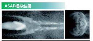
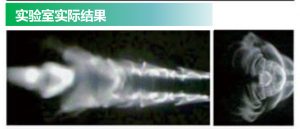
ASAP’s lamp source model is very precise in geometry and luminosity and includes complete spectral data, as well as actual optical and mechanical geometry derived from the lamp source. Light can be reflected, deflected, or scattered by the lamp source geometry. ASAP’s lamp source model takes into account the interaction of these optics, which can cause unwanted stray light on optical systems. The rigorous and accurate lamp source model is the guarantee of reliable and accurate simulation results!
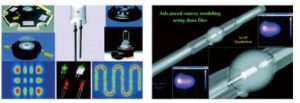
Infrared lens design software SYNOPSYS
SYNOPSYS Lens Design Software is one of the most powerful lens design software in the world today. 37 years of development updates and a Windows interface make it easy for novices to get started; it’s easy to face higher professional demands. The developer OSD has extensive experience in almost all types of optical system design, including test instruments, astronomy, lighting, low-light night vision, infrared systems, eyepieces, etc. The user’s design needs can be quickly and efficiently solved; concept development or scheme development; detailed lens design; tolerance analysis; technical performance analysis (including diffraction effects, tolerance budget impact through MonteCarlo); the established lens system automatically matches the optical sample list of preferred suppliers, thereby reducing processing costs and speeding up the design process.

- Powerful optimization features:
SYNOPSYS has the most powerful optimization capabilities to optimize optical systems quickly and accurately.

- Wide range of applications:
SYNOPSYS can analyze and optimize a wide variety of complex optical systems. Support a variety of special optical surfaces such as diffractive optical components, complex aspheric, freeform design, a variety of zoom lenses, scanning systems. It is easy to achieve the eccentricity and tilt of the components; since 1976, users around the world have successfully developed a large number of lenses using SYNOPSYS designs, which have been affirmed and praised by the majority of customers.

- Lens search function:
Enter the parameters of the system you want to design, such as wavelength, relative aperture, field of view, etc., and the software can find the corresponding structure from the built-in lens library to choose from.
- Ghost and cold reflection analysis:
Ghost images in optical systems cannot be ignored in high-end optical designs, while cold reflection is a phenomenon unique to infrared scanning imaging systems with cryogenic receiving elements. Synopsys provides four analytical calculation methods that allow users to quickly identify problem surfaces that are causing more severe ghosting or cold reflections, and can automatically reduce or eliminate their impact during optimization.

- Zoom system design optimization:
The following parameters can be optimized, lens spacing, lens radius, material, wavelength, pupil size, field of view range, etc.; the cam curve can be directly output.
- Powerful lens edge handling:

- Powerful tolerance allocation:
State-of-the-art and complete tolerance analysis program for tolerance assignments on diffraction messengers, root mean square wave aberrations, or user-defined evaluation metrics. It has the functions of automatic drawing of templates, international standard processing drawings, cost estimation and so on.

Semiconductor simulation – laser design analysis software
SimuLase™ is the first semiconductor simulation software that allows users to take full advantage of the latest semiconductor models. The software’s fully microscopic multibody model can be used to accurately verify/predict key photoelectric properties of certain structural parameters, such as gain/absorption, refractive index, spontaneous radiation (photoluminescence) or carrier losses caused by radiation and Auger losses, saving time and expensive experimental research costs.
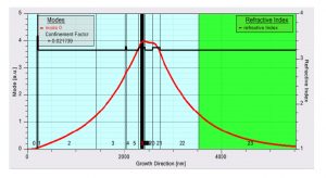
Tools for microscopic property calculation can also calculate some macroscopic characteristics of the V(E)CSEL structure, such as horizontal and longitudinal mode modes, reflection and transmission spectra, surface PL spectra considering cavity effects, threshold currents or operating characteristics, etc. Simulase simulations allow experimental results to be compared with theoretical values. Innovative research using microscopic multibody models has been demonstrated in numerous papers. SimuLase also provides examples of design, analysis, and optimization.
SimuLase™ offers:
- The software gives the exact initial basic input when modeling any trusted device. This data can also be imported into other commercial software tools for further study;
- The software gives an easy-to-use GUI interface that can determine the basic characteristics of many structures without any experimental feedback;
- The software gives a number of experimentally validated models that have been studied in more than fifty published papers over the past two decades. And, even if you’re not an expert in microscopic multibody physics, you can take advantage of this software. SimuLase can take advantage of parameter matching of microscopic multibody models to automatically design and preset all parameters. At the same time, in order to quickly browse or find out the research points of interest, the software also allows to change the calculation parameters or use simplified models.
The GUI interface adopted by this software can:
- For the design of heterogeneous structures, simply add/remove/change the width and composition of each layer;
- Instantly display the energy bands, potential energy, substrips and wave functions of heterojunction structures, calculate and display background refractive index profiles, cross-mode and longitudinal modes, and optical constraint factors;
- Calculate and display reflection and transmission spectra of structures;
- Calculate the electric field distribution of the pressure doping layer;
- Calculate the potential energy change due to the local charge inhomogeneity caused by the free carrier;
Gain Databases Gain Database:
- The database gives data for standard III-V and II-VI group element systems;
- The material properties in the database can be used to realize a complete closed-loop design of the laser chip, starting from the general structural design (such as layer width, composition and doping composition), and then predicting the excitation wavelength to the input and output characteristics within the experimental error range. The quantitative calculations provided by the software estimate the major material properties of most optoelectronic devices such as semiconductor lasers, optical amplifiers or modulators. Relative to material and structural design, these analytical results are universal and have little limitation. Using the microscopic multibody calculation process, it can be calculated:
- Gain, absorption and refraction spectra; spontaneous radiation (photoluminescence) spectra;
- Current loss of spontaneous radiation; current loss of auger process; in-band (free carrier) absorption; and related parameters such as differential gain and lineweight reinforcement factor can also be obtained.
- The algorithms used include phase shift multiplication and linear functions, avoiding complex algorithms.
OptiSystem, an optical communication system and amplifier design software
The OptiSystem is widely acclaimed for minimizing time requirements and the costs associated with the design of optical systems, links and components in areas where cost-effectiveness and productivity are critical. OptiSystem is an innovative, fast-growing and powerful software design tool that allows users to plan, test, and simulate virtually any optical link in the broad-spectrum physical layer of many optical networks, from LAN, SAN, MAN to ultra-long distances. It provides transport layer optical communication system design and planning from the component to the system level, and can visualize the analysis and scenario. OptiSystem integrates with design tools for other Optiwave products and industry-leading electronic design automation software to accelerate time to market and shorten payback periods.

Specific benefits
- Provides 360-degree insight into system performance to evaluate parameter sensitivity to assist in tolerance specification design
- Design options and scenarios can be visualized for potential customers
- Enables direct access to a wide set of system feature datasets
- Provides automatic parameter sweeping and optimization
- Can be integrated with the Optiwave family of products
apply
Developed specifically to address the needs of scientists, optical communication engineers, system integrators, academics, and many other users, OptiSystem is a powerful and easy-to-use optical system design tool that meets the requirements of the evolving photonics industry market.


